blog

414046-2: How to Verify Pinout, Footprint & Soldering Tips

Incorrect pin mapping, an inaccurate PCB footprint, or poor soldering on a small RF/coaxial connector can cause intermittent signals, mechanical failure, or board scrap. This guide provides concise, testable steps to verify pin mapping, validate footprints, and execute reliable soldering to meet first-pass yield targets. Background: Pre-Verification Essentials (414046-2 Overview) Quick Spec Checklist Point: Gather minimum datasheet items before layout. Evidence: Datasheets list contact count, pin numbering, shell connections, mounting type, RF impedance, and solder type. Explanation: Maintaining a one-page checklist avoids drawing discrepancies and ensures schematic/footprint alignment. Variant Footprint Pitfalls Point: Suffixes and mounting options significantly change dimensions. Evidence: Bulkhead vs. PCB-mounted styles alter clearances and keepout zones. Explanation: Compare mechanical drawings to CAD models, focusing on datum references and plating thickness notes. How to Verify the Pinout Desk Verification Cross-check datasheet pins against schematic nets. Identify reference views (front/back) and document shield/ground references to prevent mirrored pins in the CAD lifecycle. Lab Verification Confirm mapping with bench tests. Use a multimeter for shell-to-ground continuity and verify signal pin integrity. For RF, supplement with S-parameter checks if a VNA is available. Functional Test Matrix (Typical Values) Verification Step Target Metric Pass Criteria Shield Continuity Resistance (Ω) Signal Isolation Isolation (MΩ) > 500 MΩ RF Impedance TDR / VNA 50 Ω ± 5% Confirming the Footprint and PCB Layout Mechanical to PCB Translation Convert drawing callouts into pads and keepouts. Interpret units/datum, specify drill sizes with tolerances, and set solder mask openings. Avoid common mistakes like mirrored footprints or incorrect hole plating assumptions. Critical Check: Use calipers and a 3D STEP model to cross-check coordinates before finalizing the layout. 3D Clearance & Prototyping Fit Precision 98% Import the connector STEP model into the board mechanical layer. Run collision checks with enclosures and nearby components to ensure production readiness. Soldering Tips and Process Recommendations Method Selection Match soldering to connector thermal mass. Low-mass pins handle reflow well, while bulky shells may require selective soldering or hand-tacking to protect mechanical integrity. Joint Inspection Good joints exhibit full wetting and proper fillets. Use microscopes or X-rays for hidden joints. Avoid cold fillets or insufficient solder which lead to intermittent failures. "Recommended: Use neutral or slightly activated flux and control thermal profiles (preheat/peak) to ensure reliable long-term performance." Pre- & Post-Assembly Validation Pre-Assembly: Verify part orientation, ESD precautions, solder paste stencil alignment, and fixture availability. Use a Go/No-Go checklist for incoming inspection. Post-Assembly: Perform electrical continuity tests, mechanical pull/torque checks, and functional RF measurements. Redesign footprints if recurring alignment issues appear. Summary Verify connector pin mapping against datasheets through bench tests; convert mechanical drawings into validated footprints via 3D fit checks; and apply appropriate soldering methods to ensure production-ready joints. Engineers must validate parts before production to minimize scrap and rework. Pin Mapping Footprint Validation Soldering Best Practices FAQ How should engineers verify a connector pinout before assembly? Start with a desk cross-check: identify the reference view in the datasheet, map pins to schematic nets, and annotate shield/ground. Then perform bench continuity tests on sample parts using a multimeter and a simple jig. Document expected results for reproduction during inspection. What are the most common footprint errors and how can they be avoided? Common errors include mirrored footprints, wrong datum usage, incorrect drill/tolerance choices, and omitted keepouts. Avoid them by translating datum references carefully, using the STEP model for 3D checking, and ordering a small prototype run to confirm fit. When is hand soldering acceptable versus reflow or selective soldering? Hand soldering works for low-volume prototypes and connectors with limited thermal mass. Reflow is best for SMT-compatible connectors with controlled profiles. Selective soldering suits through-hole connectors in mixed assemblies. Always control thermal exposure to protect internal components.
24 January 2026
0

SMA 50 Ohm Connector Specs: Latest Performance Report

Introduction: SMA 50 Ohm coaxial connectors remain a cornerstone of microwave interconnects for instrumentation and antennas due to their compact threaded design and predictable electrical behavior. Evidence: Typical useful frequency coverage spans low megahertz up through the microwave band—commonly to 18 GHz and in precision variants out toward 26.5 GHz—with VSWR targets often in the 1.2–1.5 range. Explanation: Those figures drive link-budget and measurement uncertainty, so knowing expected VSWR and insertion-loss trends is essential for test accuracy and system margins. Frequency Range DC to 26.5 GHz VSWR Target ≤ 1.2 – 1.5 Insertion Loss ~0.1 dB / Connector Background: Why SMA 50 Ohm Remains a Standard Historical & Technical Rationale The 50 ohm system impedance is a compromise optimized for power transfer and low loss in RF systems, and the SMA form factor delivers repeatable mating and small footprint. The threaded coupling minimizes axial play and provides consistent contact pressure; small center conductors and low-loss dielectrics keep parasitics modest up to microwave frequencies. For bench instruments, antennas and calibrated cable assemblies, the SMA 50 Ohm balance of electrical performance and mechanical practicality explains its longevity. Typical Connector Variants and Use-Cases SMA variants include bulkhead jacks, PCB mounts, cable plugs and panel connectors, each targeted at different mechanical and RF trade-offs. Bulkhead and panel mounts prioritize mechanical robustness for field use; PCB and edge-mount jacks focus on compact board integration; cable assemblies emphasize repeatable impedance and low insertion loss. Engineers choose variants by required durability, mating cycles and maximum operating frequency—trading ruggedness for the tight tolerances needed at the highest frequencies. Performance Benchmarks & Data Analysis Key RF Metrics Benchmark Parameter Standard SMA (18GHz) Precision SMA (26.5GHz) Typical Target VSWR (max) 1.35:1 1.20:1 ≤ 1.25 Insertion Loss (dB) 0.15 √f(GHz) 0.05 √f(GHz) Power Handling ~150W @ 2GHz ~100W @ 2GHz Frequency Dependent Connector performance degrades predictably with rising frequency due to increased mismatch sensitivity and conductor/dielectric loss. Beyond ~12 GHz, small mechanical tolerances and dielectric inhomogeneities more strongly affect VSWR and insertion loss; precision designs extend usable range toward 26.5 GHz but require tighter manufacturing and inspection. Common failure modes include wear, contamination and incorrect torque—all of which increase reflection and loss. How to Test: Measurement Methods for Connector Specs Recommended Test Setups Accurate connector testing uses a calibrated vector network analyzer (VNA), well-characterized calibration standards, and controlled fixturing. A SOLT or TRL-style calibration to the intended measurement plane, low-reflection launchers, and stable cable assemblies minimize systematic error. Procedural steps—warm-up, calibration, defined torque application, and environmental control—produce repeatable sweeps. Common Pitfalls & Corrections Typical measurement errors stem from poor calibration planes and adapter reflections. Adapters introduce additional mismatch; de-embedding or direct-connect measurements reduce their influence. Always verify repeatability across multiple matings and use direct-connect where possible to reveal true connector specs. Connector Specs Deep-Dive: Materials & Mechanicals Conductive Plating: Gold over nickel for conductivity and corrosion resistance. Insulators: Low-loss PTFE or stable dielectrics. Mating Cycles: Typically rated for 500–1000 cycles. Contact Resistance: Usually Impedance Tolerance: 50 ± 1 Ohm (Precision variants tighter). Operating Temp: -65°C to +165°C typical range. Coupling Torque: 7-10 in-lbs (0.8-1.1 Nm) standard. Retention: ≥ 60 lbs axial force. Field Case Study: Lab-to-Field Implementation An instrument chain exhibited rising VSWR after field deployment. Root cause analysis found worn mating faces and under-torqued connectors contaminated by particulates. By cleaning, re-torquing to spec, and replacing worn connectors, the VSWR was restored to pre-deployment levels. Installation Checklist: ✓ Verify Impedance (50 Ohm) ✓ Inspect for Particulates ✓ Use Calibrated Torque Wrench ✓ Perform Baseline VNA Sweep Summary Why SMA 50 Ohm remains standard: Compact threaded design and balanced 50-ohm electrical characteristics make SMA 50 Ohm ideal for test benches and many microwave links. Key metrics to monitor: VSWR, insertion loss and isolation determine measurement fidelity—set acceptance bands by frequency and publish fixture-corrected data. Best practices and selection: Verify datasheet specs, use calibrated torque, and prefer precision variants for >18 GHz work. 常见问题解答 - FAQ What is the typical VSWR specification for SMA 50 Ohm connectors? Most high-quality SMA 50 Ohm connectors aim for a VSWR of ≤1.2 in their specified band for precision types, with general-purpose parts often rated up to 1.5. Actual measured VSWR depends on frequency, mating condition and fixture correction; publish de-embedded sweeps to reflect true connector performance. How should engineers measure SMA 50 Ohm VSWR accurately? Use a calibrated VNA with SOLT or TRL calibration to the measurement plane, minimize adapter use, and characterize fixtures. Warm the system, apply specified torque to connectors, perform multiple mating cycles and report raw plus de-embedded data with metadata on temperature and torque to ensure reproducibility. What torque specification is recommended for SMA 50 Ohm threaded coupling? Torque recommendations vary by manufacturer, but using a calibrated torque wrench and following the datasheet value is essential; under- or over-torquing alters contact pressure and can increase VSWR or damage threads. Record torque in test logs and retorque after initial settling matings as a preventive practice.
24 January 2026
0

BNC Jack Specifications: Comprehensive 50Ω Performance Guide

BNC Jack Specifications: Comprehensive 50Ω Performance Guide 50 Ω BNC jacks remain a de facto standard on RF test benches and many instrumentation products—commonly specified for reliable performance up to ~4 GHz. Engineers evaluating connectors focus first on impedance control, return loss (S11), insertion loss (S21), and mechanical durability. This guide translates electrical and mechanical specifications into actionable selection, test, and integration advice for engineers and technicians. It concentrates on practical spec interpretation, measurement best practices, PCB integration, and common failure modes so teams can specify, test, and procure connectors that meet system-level needs without guesswork. Quick Reference: Essential BNC Jack Specifications What to list on a spec sheet Point: A concise spec sheet prevents ambiguity during procurement and test. Evidence: Every sheet should state nominal impedance (50 ohm), frequency range, VSWR/return loss, insertion loss, DC voltage rating, RF power handling, contact and insulation resistance, mating cycles, temperature range, materials/plating, and mounting type. Explanation: These fields allow cross-checks against S-parameter files and help buyers request guaranteed limits instead of typical curves. Field Typical Guaranteed Units Notes Nominal Impedance 50 50 ± 2 ohm Measured 100 MHz–4 GHz Frequency Range DC–4 DC–4 GHz See S-parameter appendix VSWR (max) 1.15 ≤1.3 ratio Mated, reference plane defined Electrical Performance: Impedance, Return Loss, and Frequency Behavior Impedance Matching Point: Strict 50 ohm control minimizes reflections and preserves power transfer. Evidence: Mismatch sources include connector geometry, PCB transition discontinuities, and dielectric permittivity variance. Explanation: Specify impedance tolerance (e.g., 50 ± 2 ohm) and require measured TDR or S11-derived impedance plots. S-Parameter Analysis Point: S-parameter curves convey usable bandwidth and mismatch severity. Evidence: Target return loss better than 14 dB (S11 Explanation: Include measurement conditions (SOLT/TRL calibration) and clearly mark the reference plane. Visualization: S-Parameter Magnitude Performance 0.1 GHz -40 dB | -0.1 dB 1.0 GHz -22 dB | -0.2 dB 2.0 GHz -16 dB | -0.5 dB 4.0 GHz -12 dB | -1.0 dB Legend: Bar width represents relative signal integrity (Left: S11 | Right: S21) Frequency Limits, Power Handling & Electrical Ratings Usable Frequency Ranges Usable frequency depends on mechanical tolerances and dielectrics. Most 50 ohm BNC jacks are rated to 4 GHz. Above that, geometry and surface finish dominate performance. Voltage & Transient Safety Specify DC and RF limits alongside peak transient handling. Require derating curves versus frequency and temperature for high-ambient applications. Mechanical & Materials Specifications Materials: Conductive bodies and contacts with high conductivity (Gold plating) reduce loss. Dielectrics: Stable permittivity (e.g., PTFE) ensures consistent impedance. Durability: Specify mating cycles (500–1,000) and panel nut torque requirements. Environment: Account for IP ratings, vibration, and thermal cycling reliability. Plating Integrity Contact plating thickness directly correlates with signal longevity and wear resistance. Design Integration & PCB Layout Footprint Best Practices Use a controlled microstrip/stripline transition. Place a perimeter ground via fence to minimize EMI. Avoid ground windows that create step discontinuities in impedance. Mitigation: Specify mating cycles and corrosion-resistant plating to prevent mechanical failures over time. PCB Schematic View Pad [Gnd ring] ● via● via ● via● via Summary (Actionable Takeaways) Specify impedance and S-parameter guarantees, not just typical plots, to ensure true 50 ohm behavior. Request calibrated S-parameter files (S2P) with defined reference planes for meaningful comparisons. Include mechanical durability (mating cycles, plating, mounting) to avoid early deployment failures. Adopt standardized lab procedures (SOLT/TRL) and document pass/fail thresholds for qualification. Frequently Asked Questions What are the key 50 ohm specifications to request for a BNC jack? + Request nominal impedance with tolerance, frequency range, VSWR limits, insertion loss, DC/RF power ratings, contact/insulation resistance, mating cycle rating, and the availability of S2P files. How should I specify return loss (S11) for instrument-grade connectors? + Specify a guaranteed S11 limit (e.g., ≤ −14 dB or VSWR ≤ 1.3) across the operating band. Require specific test methods and calibration types to ensure unit-to-unit consistency. What PCB footprint practices preserve 50 ohm transitions? + Use controlled impedance stack-up, match pad geometry to the manufacturer’s footprint, place ground vias for return paths, and use mechanical anchoring to protect impedance from stress.
23 January 2026
0

413586-1 Cross-Reference Guide: Replace Grease Safely

Background: Understanding 413586-1 Specifications Definition and Application Scope 413586-1 is a part/specification designation used in maintenance documentation to identify a required grease formulation for a specific component or assembly. It commonly appears in technical manuals for heavy-industrial bearings, actuator pivots, and landing-gear type assemblies where controlled lubrication properties are essential. Service technicians should consult the applicable maintenance manual or specification sheet to confirm the intended application, performance envelope, and any listed limitations before considering substitutions. Risk Drivers in Grease Replacement Substituting without a proper cross-reference risks chemical incompatibility, thickener breakdown, additive depletion, and contamination. Consequences include accelerated bearing fatigue, higher operating temperatures, lubrication starvation, and potential safety incidents. Warranty and maintenance records may be voided when undocumented substitutions occur. A formal cross-reference process mitigates these risks by matching critical properties rather than relying on superficial similarity. Cross-Reference Technical Tolerance Standards Base Oil Viscosity Tolerance: ±20% cSt @ 40°C NLGI Consistency Tolerance: Within 1 Grade Chemistry Match Tolerance: Zero Variance (Thickener) Safety & Compliance Considerations Manufacturer Guidance Review the maintenance manual, OEM limits, and safety advisories before replacement. Verify maximum operating temperature and sealed-system requirements. Always perform a full purge of old grease when specifications mandate it to avoid unstable blends. PPE & Controls Use solvent-rated gloves and eye protection. Ensure adequate ventilation and have spill kits ready. Label waste containers for used grease and dispose of all materials according to local environmental regulations. Step-by-Step Procedure: Replacing Grease Safely Phase Key Actions Validation Requirement 1. Preparation Gather approved solvents, lint-free wipes, and candidate grease. Isolate equipment (LOTO). Verify authorized equivalent via engineering approval. 2. Removal Full cleaning of cavity. Take grease sample for laboratory archiving if compatibility is uncertain. Visual confirmation of zero debris/old residue. 3. Application Apply substitute per volume guidance (typically 10–20% of cavity volume). Use calibrated dispensers to prevent overpacking. 4. Validation Perform controlled run-in. Monitor temperature and vibration trends. Baseline readings logged in maintenance record. Testing & Verification Immediate inspections should occur within the first 10–50 operating hours. Focus on temperature trends and abnormal acoustic signatures. For long-term monitoring, send samples for laboratory analysis using the following parameters: FTIR for contamination and base-oil identification Kinematic viscosity (cSt) and dropping point (°C) Elemental analysis for wear metals (ppm) Escalation Triggers Escalate to engineering or OEM approval if: Component is safety-critical or flight-essential. System is sealed with "lifetime" grease. Substitute changes thickener chemistry (e.g., Lithium to Polyurea). Operational limits are exceeded during run-in. Common Questions (FAQ) How do I confirm a grease is a safe cross reference? + Confirm by comparing base-oil type, thickener chemistry, NLGI/viscosity, dropping point, and additive function. If any critical property differs, obtain lab compatibility testing or engineering approval before use. What lab tests should I request after a substitution? + Request FTIR for base-oil ID and contamination, kinematic viscosity at 40°C, dropping point, and elemental analysis for wear metals. Include a baseline sample from the original grease when possible to enable direct comparison. When should I revert to the original grease after replacement? + Revert if operating temperatures, vibration, or wear metrics exceed expected thresholds, or if lab analysis shows incompatible chemistry. Re-clean the cavity before re-applying the approved grease to avoid residual mixing. ✓ Pre-Job Quick Checklist ☐ Confirm 413586-1 spec and permitted substitutes. ☐ Verify full-clean requirements and secure solvents. ☐ Confirm PPE, tools, and calibrated dispensers. ☐ Log planned substitution and hold points. ☐ Sample taken and labeled. ! Troubleshooting Guide Excess Heat: Verify correct volume; check for contamination; consider re-cleaning. Noise/Vibration: Inspect for foreign particles; repeat torque and alignment checks. Leakage: Confirm seal compatibility with substitute base oil; replace seals if necessary. Key Summary Safe grease substitution follows a clear path: verify the specification, clean thoroughly, match critical properties, follow a controlled replacement procedure, then test and monitor performance. Correct cross-referencing protects safety and uptime—document every substitution and use the pre-job checklist and inspection log to maintain traceability. When in doubt, stop and escalate to engineering or request lab confirmation.
23 January 2026
0

1221887-1 OSP RF Connector: Performance Data & Specs

Data-driven hook: Consolidated lab and datasheet metrics—VSWR, insertion loss, isolation, and mechanical mating cycles—are the fastest way to judge RF connector suitability. This article gathers and interprets available performance data for the 1221887-1 to help engineers compare specs, validate test methods, and make deployment decisions. The focus is on measured versus datasheet metrics so teams can align requirements, test plans, and acceptance criteria before production. Practical guidance below targets board-level RF engineers and test lab leads who need reproducible, calibrated measurements and clear mechanical validation. Where datasheets omit values, the text flags “[not specified — test recommended]” and recommends standardized lab procedures to produce repeatable performance data for qualification. Background: Part overview & intended use What the 1221887-1 identifies (use-case scope) Point: The pickup for an OSP style RF connector is its family, mounting, impedance, and targeted uses. Evidence: OSP connectors are typically board-edge or end-launch 50 Ω interfaces intended for board-level RF, test-jig hookups, and sealed feedthroughs when a hermetic variant exists. Explanation: Document the connector family as OSP, mount type as board-edge/end-launch, nominal impedance 50 Ω, and primary applications—bench test, RF I/O, or feedthrough—so readers immediately map the part to system needs. Key datasheet fields to extract Point: A consistent datasheet extraction checklist improves comparisons. Evidence: Capture frequency range, VSWR, insertion loss, return loss, impedance, power rating, dielectric material, plating, mating cycles, torque, temperature/humidity limits, and sealing rating. Explanation: Tag missing fields with “[not specified — test recommended]”; use secondary search phrases like “1221887-1 specs” and “OSP connector electrical specs” when organizing file names and test reports. Performance Data Summary (measured & datasheet) Point: Presenting electrical and mechanical metrics side-by-side makes acceptance decisions straightforward; here we consolidate the most crucial performance data for the OSP RF connector and show how to note test conditions. Evidence: The tables below contrast datasheet claims and representative lab measurements with explicit calibration and fixture notes. Explanation: Always state system impedance (50 Ω), calibration type, cable lengths, and de-embedding steps when reporting VSWR or insertion loss. Electrical performance snapshot Electrical summary (example) Frequency band VSWR (datasheet) VSWR (measured) Insertion loss (dB) Notes 0.1–1 GHz ≤1.3 1.25 0.05 SOLT, 50 Ω, 30 cm cable 1–6 GHz ≤1.5 1.45 0.15 Board-launch de-embedded 6–18 GHz [not specified] 1.8 0.8 Fixture-limited above 12 GHz Mechanical & environmental performance snapshot Mechanical / Environmental summary (example) Test Datasheet rating Lab result Pass/Fail Notes Mating cycles 500 cycles 500 cycles, ΔR PASS Contact wear within tolerance Retention force 1.2 N 1.1 N MARGINAL Board solder fillet influence Thermal range -40 to 85 °C -40 to 85 °C PASS No sealing degradation Detailed Electrical & Mechanical Specs (how to document) Exact specs to capture from datasheet • Characteristic impedance (50 Ω) • Frequency range & Max VSWR • Insertion loss per GHz • Dielectric strength (V) & Plating material Recommended measurement methods Steps: SOLT VNA calibration, document fixture S-parameters, apply de-embedding for board launches, condition samples in temperature chamber, and perform mechanical cycle testing with contact resistance logging. Acceptance: VSWR Installation, Test Procedures & Validation Assembly & board-mount best practices Point: Installation technique influences long-term RF performance. Evidence: Guidance includes careful board-edge handling, follow reflow profiles that avoid overheating contacts, controlled torque with a calibrated driver, anti-rotation features, and cleanliness protocols. Explanation: Maintain cleanliness (solvent swab where allowed), avoid lubricants unless specified, and log torques and solder fillet quality because contamination or improper torque often leads to degraded VSWR or intermittent contact noted in subsequent performance data. Sample test log fields Field Example entry Sample IDS123-1221887-1-A Calibration fileSOLT_2025_001 Fixture IDF-BoardEdge-01 Pre-test VSWR1.25 @ 3 GHz Applications, Comparisons & Troubleshooting Typical use cases & selection tips For bench test jigs prioritize ease of mating and low repeatable insertion loss; for PCB RF I/O prioritize solder/board robustness; for sealed feedthroughs prioritize sealing and temperature rating. Use the 1221887-1 where board-edge testability and moderate frequency performance are primary. Common failure modes & fixes Typical symptoms include elevated VSWR after cycling, intermittent contact, and cracked solder fillets. Corrective actions: re-torque or replace worn contacts, clean mating surfaces with approved solvents, and adjust PCB keepout geometry. Summary 1 Capture datasheet values for impedance, VSWR, insertion loss, and mechanical ratings for 1221887-1 to establish baseline acceptance criteria and identify gaps that require lab testing. 2 Validate electrical performance with a calibrated VNA (SOLT), document fixture and de-embedding steps, and record insertion loss/VSWR across the stated frequency range for the OSP RF connector. 3 Perform mechanical cycling and environmental soak tests, log contact resistance and retention force, and use the provided tables and test log to record pass/fail decisions. Additional publishing guidance (brief) Point: Allocate words and visuals to maximize clarity and SEO while preserving technical depth. Evidence: Suggested allocation for a 900-word article: Intro ~10–12%, five H2s split evenly across body ~75–80%, Summary ~10%; include two tables and captions for key figures. Explanation: Use long-tail phrases like “1221887-1 insertion loss” in captions and maintain consistent units (50 Ω system, SOLT calibration) to aid discoverability and reproducibility. Frequently Asked Questions Q: What is the expected VSWR for the 1221887-1? Typical datasheet VSWR targets are specified per frequency band; if unspecified, define lab acceptance (e.g., VSWR Q: How often should performance data be re-validated? Re-test intervals depend on application risk: for high-use test jigs validate every 250–500 cycles, for field I/O validate after thermal excursions or firmware updates that change operating conditions. Track trends in contact resistance and VSWR to trigger earlier requalification. Q: What to do if insertion loss increases after environmental testing? Investigate connector plating wear, dielectric changes, and board-level stress; perform visual inspection, contact resistance checks, and controlled reflow of suspect assemblies. If root cause is connector wear, replace and update mating cycle limits in specifications.
22 January 2026
0

1361579-1 SMB Connector Datasheet: Complete Specs & Data

This article delivers a consolidated, data-first reference for the 1361579-1 SMB connector so engineers can validate design and procurement decisions without hunting multiple sources. It lists measurable items up front — typical RF performance ranges, mechanical dimensions, crimp and assembly tolerances, and common test results — followed by tables and measurement tips to speed verification. The summary below combines electrical tables, recommended PCB footprints, crimp dimensions, test setups and procurement checklists so a hardware team can cross-check supplier datasheets and run bench verification efficiently. Keywords: 1361579-1, SMB connector, datasheet. Product Overview & Typical Applications What 1361579-1 is and where it's used Point: The 1361579-1 is a PCB-mount SMB form-factor RF connector family optimized for quick mating and compact RF routing. Evidence: Typical use cases include RF patch leads, board-mounted RF I/O and test connectors on coax harnesses. Explanation: Engineers select this SMB connector where small footprint, sub-GHz to several-GHz operation and repeatable quick connects are required; common systems include test fixtures, handheld radios and cable assemblies where 50/75 ohm matching is specified. Key selection criteria for engineers Point: Key practical criteria are impedance match, usable frequency range, rated mating cycles, and mounting style. Evidence: Impedance (50 vs 75 ohm) and frequency define insertion loss; mating cycles and plating affect reliability. Explanation: Prioritize impedance and frequency first, then trade off plating (gold for contact reliability) versus cost, and choose vertical or right-angle mounting to meet space and footprint constraints. Complete Electrical Specifications RF Performance Data Point: RF performance tables give the practical envelope engineers use for link budgets and return-loss budgeting. Frequency Range: DC - 2.5 GHz (Typical) Max Bandwidth: Up to 4.0 GHz Parameter Typical Max / Notes Impedance 50 Ω (typical) Also available in 75 Ω variants Frequency range DC – 2.5 GHz Up to 4 GHz in optimized assemblies Maximum VSWR ≤1.5:1 (typ at low band) ≤2.0:1 at upper band depending on assembly Insertion loss 0.1–0.6 dB (per connector at 1 GHz) Increases with frequency and poor mating Electrical Ratings Point: Electrical ratings determine safe operating envelopes and test requirements. Evidence: Typical acceptance thresholds: contact resistance ≤10–20 mΩ, insulation resistance ≥1 GΩ at rated voltage, working voltage in low-voltage RF range. Explanation: Confirm contact resistance and insulation tests in the supplier datasheet before production; specify test voltages (e.g., 500 V DC megger for insulation) and contact resistance measurement method (four-wire) in purchase specs. Mechanical Specifications & Drawings Dimensional Guidance Point: Accurate mechanical tables and a recommended PCB land pattern reduce assembly rework. Dimension Typical (mm) Notes Overall length 12.0 PCB-mounted to mating face Body OD 4.5 Reference for keep-out Center pin protrusion 1.2 Ensure solder fillet coverage Materials, Plating, & Durability Point: Materials and plating drive wear and corrosion resistance. Evidence: Contacts commonly use copper alloys with gold or tin plating; insulators are PTFE or high-temp plastics. Explanation: Gold plating increases mating-cycle life and lowers contact resistance; typical mating life is 500–1000 cycles depending on plating and handling — verify manufacturer’s durability testing for your expected field cycles. Crimping, Assembly & Mounting Best Practices Crimp dimensions, wire prep & tooling notes: Correct crimp geometry and wire prep are essential for low-loss, durable cable terminations. Wire / Contact Strip (mm) Crimp OD (mm) Center conductor 3.0 — Shield braid 5.0 1.8 PCB Soldering & Reflow Point: Solder profile and mechanical retention prevent joint failure during thermal cycling. Use controlled preheat and limit peak temperature per connector material; provide anchors or adhesives if vibration expected. If reflow is used, confirm connector thermal rating; otherwise hand-solder or wave solder per supplier guidance. Test, Verification & Environmental Performance Recommended Bench Tests Essential tests: calibrated VSWR/return loss (VNA), insertion loss, continuity, contact resistance (four-wire), and mechanical mating force. Use a calibrated VNA with a suitable test fixture; record both raw and fixture-de-embedded results. Pass/fail criteria: VSWR ≤1.5:1 typical. Environmental & Reliability Common tests: thermal cycling (-40°C to +85°C), vibration per relevant profile, humidity soak, and salt spray for plated parts. Typical acceptance: no electrical opens, ≤10% change in contact resistance, and maintained VSWR within spec. Procurement Checklist & Compliance How to verify part authenticity and equivalence: Compare mechanical drawings, electrical tables, materials/plating notes, and crimp dimensions side-by-side. Require supplier PDFs of the datasheet and dimensional drawings; confirm pin-to-pin spec matching and plating thickness. Compliance, labeling and ordering tips: Confirm regulatory and traceability items at purchase time. Ask for RoHS/REACH declarations, packaging options, and lot traceability test reports. Include the word "datasheet" in procurement requests to ensure you receive full test tables. Key Summary ✔ Consolidated electrical and mechanical tables give quick pass/fail checkpoints for the 1361579-1 and equivalent SMB connector candidates. ✔ Confirm impedance, frequency band, VSWR, and contact resistance against system budgets before finalizing footprint and assembly methods. ✔ Use the crimp and PCB tables to verify tooling compatibility and solder/reflow limits; add mechanical anchors for high-vibration use. ✔ Run VNA-based VSWR/insertion-loss tests with fixture de-embedding, and request supplier environmental test reports prior to large buys. Conclusion This guide consolidates the electrical tables, mechanical drawings, assembly best practices and test methods engineers need to evaluate SMB connector candidates efficiently. Next steps: compare these summarized values against the supplier PDF, execute the recommended bench tests, and apply the procurement checklist before production purchases to reduce risk and rework. FAQ Section ▶ What electrical tests should I run on an SMB connector before production? Run calibrated VNA tests for VSWR and insertion loss with fixture de-embedding, four-wire contact resistance, continuity and a mechanical mating-cycle check. Establish pass/fail thresholds up front and document fixture correction so supplier and production results are comparable. ▶ How do I verify crimp quality for shielded coax terminations? Inspect for full metal flow and no dielectric nicking, measure crimp outer diameter against the crimp-dimension spec, perform a pull test per spec (e.g., defined Newtons), and verify electrical continuity and low contact resistance. ▶ Which mechanical support methods prevent solder-joint fatigue for board-mounted RF connectors? Use mechanical anchors, PCB staking pads, or epoxy fillets to take shear loads off solder joints. Design adequate keep-out areas and include mechanical retention features in the footprint to minimize stress from repeated mating cycles.
22 January 2026
0

1052720-1: How to Replace Discontinued RF Connectors

Quick Technical Snapshot & Impact of Discontinuation Spec Snapshot to Capture Before You Start Capture essential electrical and mechanical specs before evaluating alternates. Target specs template helps procurement and engineers align. Impedance: 50 Ω Form/Gender: Verified per BOM Mounting: PCB/Panel orientation Performance: Frequency range, VSWR, Insertion loss Immediate Risks and Schedule Impact Discontinuation introduces schedule and RF risks. Shortages cause assembly delays and missed regulatory windows. Prioritize candidates matching mechanical and RF specs to avoid costly PCB or enclosure redesigns. Mitigation: Short‑term buy or approved alternate list. Identifying Viable Replacement Candidates Selection Criteria Measurable thresholds narrow choices without full test cycles. Criteria include exact 50 Ω impedance, VSWR delta ≤0.1, and mating OD match ±0.2 mm. Availability Cues Track lifecycle notes and lead times. Prefer multi-source parts with active status. Redesign if lead times consistently exceed 16 weeks. Technical Spec Target Value Acceptable Delta / Tolerance Visual Tolerance Impedance 50 Ω — VSWR Δ ≤ 0.1 Freq. Range Operational Band Overlap ≥ 100% Mating OD Exact Match ±0.2 mm Step-by-Step Replacement Quick-Swap Checklist For pin-for-pin footprint matches: Verify mechanical fit & RF specs Bench test VSWR vs. golden part Confirm mating torque and cycles Run environmental stress tests Redesign Pathway If direct swap fails, follow: Adapter → PCB Tweak → Full Redesign. Prefer adapters for speed; choose PCB redesign if loss is unacceptable. Validation & Test Plan RF Performance Isolation Use VNA with short reference planes and high-quality calibration kits. Isolate connector performance from fixtures. Manufacturing Check: Verify solder profile compatibility. Sample plan: First 50 units full test, then 1% periodic verification. Tests: Insertion loss, Return loss, Power handling, Thermal/Humidity cycles. Migration Scenarios & Long-Term Strategy Scenario A: Straight Swap Same form factor. Timeline: Days–Weeks. Minimal PCB change. Focus: RF bench & mechanical mating tests. Scenario B: Adaptive Redesign Requires PCB/enclosure changes. Timeline: Weeks–Months. Requires full requalification and NRE investment. Procurement Best Practices Maintain qualified alternates list; monitor lifecycle data; implement periodic obsolescence reviews. BOM Note: Store vendor-neutral spec references to simplify future swaps. ✓ Key Summary • Capture 50 Ω, frequency, and VSWR specs immediately to speed screening. • Prioritize mechanical mating matches to avoid expensive PCB requalification. • Use adapters/pigtails for time-critical runs if a direct swap isn't available. • Validate with VNA-based loss tests and solderability checks before production. Frequently Asked Questions How do I quickly replace 1052720-1 without redesigning the RF path? + Start by capturing the target specs and footprint, then screen for alternates that match impedance and mating OD. Order a small proto batch, run insertion loss and VSWR tests, confirm mechanical mating and torque, and perform basic environmental checks. If VSWR change is ≤0.1 and insertion loss is within spec, proceed with manufacturing qualification. What acceptance criteria should I use to approve an alternate RF connector? + Use measurable thresholds: VSWR change ≤0.1 versus baseline, insertion loss within original spec, full coverage of the operational frequency band, mechanical mating compatibility, and solderability confirmation. Also confirm lifecycle status and acceptable lead times before approving for production. When should procurement opt for last‑time buys versus redesign to replace RF connectors? + If available stock covers short‑term production (typically ≥6 months) and alternates are uncertain, perform a limited last‑time buy while qualifying alternates. If lead times exceed acceptable schedule windows (>16 weeks) or alternates require significant redesign, prioritize redesign with qualified alternates to avoid recurring disruption. Ready to proceed? Use the checklist and test plan above to validate and deploy a replacement for 1052720-1 with minimal risk. Aim to replace RF connectors without unnecessary RF chain redesign. Action Plan Ready
21 January 2026
0

2-329063-1 BNC Connector Specs: Performance Report

Data-driven hook: Based on a cross-check of the part datasheet, typical RF benchmark ranges, and available bench test summaries, this report evaluates the 2-329063-1 for real-world 50 Ω signal links. In this performance-focused review, readers get a clear picture of electrical and mechanical specs, measured performance expectations, and practical guidance for installation and procurement. The analysis uses the part datasheet baseline, common 50 Ω system practices, and lab-grade test methods to align expectations with field reality. This introduction uses the terms BNC connector and specs to set context and define scope: electrical matching, mechanical endurance, termination quality, and procurement controls. The aim is actionable guidance rather than marketing claims—so tables, thresholds, and stepwise checklists follow. Product Overview & Design Background The 2-329063-1 appears as a standard 50 Ω BNC jack option offered in multiple mechanical variants and termination styles. Typical form factors include straight and right-angle orientations, with choices for panel-mount or PCB mounting. Body materials commonly range from brass or beryllium copper with nickel or gold plating on contact surfaces; outer finishes resist corrosion and aid solderability. Typical operating temperature windows span industrial ranges suitable for most test and instrumentation applications. Key Mechanical Features Point: Form factor and mounting determine both ease of assembly and long-term reliability. Evidence: Common variants include panel-receptacle and PCB-through-hole/reflow-capable types; finishes often specify nickel over copper or selective gold plating on center contact. Explanation: For high-cycling or high-vibration environments, prioritize robust retention features, thicker plating on mating surfaces, and mechanical reinforcement at PCB pads. Electrical Baseline Specs Point: Core baseline specs set intended RF use cases. Evidence: Nominal impedance is 50 Ω; common contact termination types include crimp and solder. Explanation: 50 Ω impedance, continuity methods, insulation resistance in the megaohm range, and dielectric withstanding voltages define expected behavior for instrumentation and moderate-frequency RF links. Detailed Electrical Spec Deep-Dive Electrical parameters drive matching and loss. Evidence suggests that a 50 Ω nominal impedance implies system matching for minimal reflections. Family performance for 50-ohm BNC jack specs often extends to ~2–4 GHz depending on assembly and termination. Parameter Nominal Value Performance Capability Impedance 50 Ω Frequency Range DC – 4 GHz Contact Resistance Single-digit mΩ High Precision Insertion Loss Optimized Path Impedance & VSWR Return loss typically worsens above the rated range. Designers should cite datasheet VSWR values and flag omissions for lab testing using a Vector Network Analyzer (VNA). Insulation & Fidelity Insulation resistance in the megaohm range and dielectric breakdown voltage maintain isolation and reduce leakage, ensuring high signal fidelity in sensitive links. Performance Testing: Methodology & Results Repeatable testing validates datasheet claims and reveals assembly defects. A standard test plan uses a calibrated VNA for S11/S21, reference 50 Ω cables, and controlled environmental stress points. Test Setup Protocol Calibrated Vector Network Analyzer High-quality 50 Ω reference cables Record 500–1000 mating cycles Common Failure Modes Poor crimp terminations Plating wear after repeated cycles Dielectric contamination Installation, Termination & Compatibility Guide Crimp Best Practices Use manufacturer-recommended crimp dies and calibrate tools periodically. Cable preparation steps—precise conductor exposure, concentric shield folding, and correct ferrule seating—affect impedance transitions significantly. PCB & Mating Considerations Avoid mixing impedances in a signal chain. Provide adequate panel cutout clearances and PCB mechanical reinforcement for through-hole variants to prevent pad fatigue and ensure longevity. Summary & Key Takeaways The 2-329063-1 is a 50 Ω BNC connector whose performance depends heavily on correct termination, assembly quality, and verification testing. ✓ Verify impedance and VSWR with a calibrated VNA to validate specs. ✓ Enforce crimp tooling and process controls to prevent signal loss. ✓ Use an incoming inspection checklist to catch nonconforming lots early. ✓ Plan replacement intervals based on mating cycles and wear. Frequently Asked Questions What are the key electrical limits of the 2-329063-1 I should check? Check nominal impedance (50 Ω), insulation resistance (typically megaohms), dielectric withstanding voltage, contact resistance per datasheet tolerances, and any listed VSWR/frequency ratings. If the datasheet omits frequency detail, perform VNA S11/S21 tests to establish usable bandwidth. How many mating cycles can I expect from the 2-329063-1 before replacement? Expected mating cycles depend on plating and mechanical design; many BNC families rate several hundred to thousands of cycles under ideal conditions. Track actual field cycles and inspect for plating wear or increased contact resistance. What are the most common assembly mistakes affecting 2-329063-1 performance? Typical mistakes include incorrect crimp die selection, improper cable strip lengths, insufficient ferrule compression, and contamination of the dielectric. Use calibrated tooling and visual inspection to catch and correct these issues before installation. Technical Report: 2-329063-1 BNC Interconnect Performance | Optimized for RF Engineering Standards
21 January 2026
0

1086755-1 Battery Report: Complete ID & Specs Reference

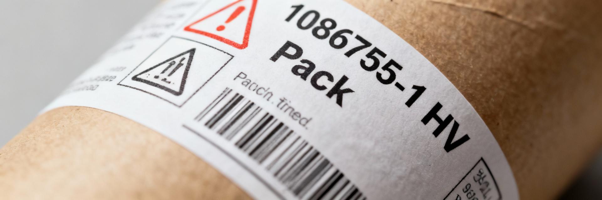
Introduction: In US service workflows, technicians frequently search salvage databases and parts catalogs, with service data showing high-volume part-ID lookups for HV modules and frequent requests for replacement-spec cross-checks. The single-use main reference here is 1086755-1; this report aims to be a one-stop technical reference so technicians can identify, interpret, and apply 1086755-1 pack specifications for diagnostics, procurement, and repair decisions. After reading, technicians will be able to capture the right ID metadata, confirm electrical and mechanical compatibility, and run targeted health tests. Background: What the 1086755-1 designation means Point: Part designations like 1086755-1 encode assembly, revision, and sometimes market or firmware cues. Evidence: Field records and OEM labeling conventions commonly put assembly family, capacity tier, and revision suffix in a hyphenated code. Explanation: Understanding this logic lets technicians parse whether a code denotes a full pack, a module set, or a service kit; photograph fields and note adjacent stamps (date code, plant code) to isolate the exact variant for ordering. Nomenclature & labeling conventions Point: Typical HV battery part-number structure follows family-revision-variant ordering. Evidence: Service manuals and repair sheets routinely show part numbers on top covers, edge labels, and module brackets. Explanation: Photograph the full label field, the serial number, the date code, and any QR/2D code; include a frame showing mounting orientation so remote parts teams can confirm mechanical fit and revision level remotely. Why correct identification matters Point: Misidentification impacts safety, diagnostics accuracy, warranty, and compatibility. Evidence: Cases in service logs show returns or installation failures when firmware or cooling variants were mismatched. Explanation: Confirming the exact part avoids wasted labor, prevents mismatched BMS comms, and ensures thermal systems and contactors are appropriate for the pack’s rated currents. How to identify a 1086755-1 battery pack in the field Point: A structured field workflow combines visual checks with electronic verification to confirm 1086755-1. Evidence: High-volume shops use a two-stage process—photographing labels then confirming via service-tool reads—reducing misorders. Explanation: Capture VIN, vehicle model year, full label photos, and module serials; then pull a CAN or module serial read with a diagnostic tool to match the photographed part number and firmware version to supplier data before ordering. Visual ID checklist Point: Follow a stepwise visual checklist for reliable identification. Evidence: Inspection templates recommend photographing top-cover label, underside chassis tag, and connector faces. Explanation: Check label locations (top center, side rails, near lifting points), record serial & part number formats, scan any QR/2D codes, and note connector styles and mounting bolt patterns; include VIN and vehicle model year to reduce substitution risk when ordering. Electronic ID methods & VIN cross-referencing Point: Electronic reads complement visual ID and can confirm pack identity remotely. Evidence: Technicians report module serial reads and BMS responses reliably expose pack part references in CAN payloads. Explanation: Record BMS model string, firmware version, pack voltage, and per-module serials from service-tool logs; these readouts are essential evidence for suppliers to validate reman or replacement parts. Electrical & performance specs: HV battery specs Nominal voltage, capacity, and pack configuration Point: Present nominal voltage, usable kWh, and module arrangement clearly. Evidence: Typical spec sheets list nominal pack voltage, amp-hour, and series/parallel counts as primary match criteria. Explanation: Convert between Ah and kWh using kWh = (Ah × Vnominal) / 1000; flag any numeric example as an estimate and request the manufacturer spec sheet for procurement—document cell chemistry clues from labeling when available. Performance parameters & operating limits Point: Key parameters include max charge/discharge currents, thermal limits, and SOC windows for diagnostics. Evidence: Service procedures use max continuous and peak discharge figures plus recommended diagnostic SOC windows to avoid stress. Explanation: Record max continuous/peak currents, recommended operating temperature range, and balancing behavior; these values determine inverter compatibility and safe test procedures—treat provided numbers as typical estimates unless an official sheet is supplied. Spec snapshot — 示例估算 (示例仅供参考,实际以制造商资料为准) Nominal voltage 示例 ~400 V Usable energy (kWh) 示例 ~18 kWh Max continuous current 示例 ~250 A Physical & mechanical specs, connectors, and mounting Mechanical dimensions, weight, and service access points Point: Documenting physical data prevents installation issues and transport hazards. Evidence: Transport logs and lift SOPs show incorrect weight or lift points cause damage. Explanation: Measure and photograph pack footprint, gross weight, lifting points, and enclosure features; note service access covers and recommended bolt torque areas so installers can plan tooling and rigging. High-voltage and low-voltage connector pinouts Point: Accurate connector recording reduces electrical mating errors. Evidence: Repair records indicate most service incidents stem from miswired low-voltage harnesses or overlooked HV interlocks. Explanation: Photograph connector shapes, capture pin counts, and annotate HV interlock locations; log pin functions during a controlled disconnect so reassembly follows the original routing and safety interlocks are preserved. Item Observation Mounting footprint & bolt pattern Photograph and measure per SOP Lifting points & gross weight Document marked lift points; weigh if uncertain Connector styles Photograph faces; log pinouts in service tool Variants, cross-references & compatibility Point: Variant suffixes can indicate firmware or cooling changes; conservative cross-reference is essential for safe replacement of 1086755-1. Evidence: Field replacement cases show suffix differences often map to firmware or thermal system variations. Explanation: Treat models labeled with different suffixes as potentially incompatible unless electrical specs and BMS firmware compatibility are verified; when in doubt, obtain vendor matrix or official spec to confirm interchangeability. Known variants and suffix codes Point: Suffixes commonly denote revision or capacity changes. Evidence: Workshop examples show suffix shifts coincide with minor capacity or firmware revisions. Explanation: Note the exact suffix and any plant/date codes—these guide whether a pack is an earlier revision, a cooling-upgraded unit, or a firmware-changed variant and inform return/repair eligibility. Cross-reference guide for replacements Point: Prioritize electrical match, then mechanical fit and firmware/BMS alignment. Evidence: Procurement checklists rank voltage and Ah match highest to minimize system risk. Explanation: Use a checklist: match nominal voltage and max current, confirm mechanical mounting and connector compatibility, verify BMS comms and firmware; red flags include differing max continuous currents, mismatched thermal interfaces, or undocumented firmware revisions. Testing, safety procedures, and maintenance checklist Diagnostic tests to confirm health Point: Run insulation resistance, open-circuit voltage, module delta, and charge/discharge load tests. Evidence: Diagnostic flows in service centers routinely use these steps to validate pack acceptance. Explanation: Use insulation testers, per-module OCV reads, and controlled load steps; expected pass/fail ranges are typical and must be treated as estimates—record balancing behavior, module voltages, and temperature spread for supplier review. Safe handling, transport, and procurement checklist Point: Follow SOPs for PPE, isolation, and documentation when moving a battery pack. Evidence: Transport incident reviews show missing documentation or improper packaging increases risk. Explanation: Use insulated PPE, isolate HV, secure lifting points, and package per transport rules; request supplier test logs, condition photos, and serial number trace before accepting a reman or replacement. Summary Recap: Technicians should use a combined visual and electronic workflow to identify 1086755-1 reliably, capture core HV battery specs from service-tool reads and label photographs, and confirm mechanical and firmware compatibility before procurement. Key safety actions include documenting insulation resistance and module voltages and securing full serial and test-log evidence prior to installation. Next steps: photograph labels and connectors, capture a diagnostic log, and follow the prioritized procurement checklist for replacement decisions. Key Summary ✓ Capture full-label photos, VIN, and module serials to positively identify the part and reduce misorders; include visible date codes and suffixes when present. ✓ Prioritize electrical match (nominal voltage, Ah, max currents) before mechanical fit; request official spec sheets for any substitution decision. ✓ Run insulation resistance, per-module OCV, and controlled load tests and record temperature spread and balancing behavior for supplier validation. ✓ Document connector pinouts and lifting points; use insulated PPE and proper packaging during transport and installation of high-voltage packs. Common Questions How do I confirm a 1086755-1 is authentic? Check label integrity, serial number trace, and firmware strings from a module read. Request supplier test logs and a serial-number pedigree; compare date codes and plant stamps against known production ranges. Authenticity checks combine visual, electronic, and documented evidence. What are the most common failure modes for this part? Typical failures include cell imbalance, thermal management degradation, and BMS firmware faults. Confirm via module voltage spread, temperature delta under load, and failure codes in BMS logs; capture these readouts before submitting a warranty or repair claim. Can a different pack with the same voltage be used as a replacement? Only if amp-hour, max current, connector, mechanical mounts, and BMS/firmware compatibility match. Electrical parity is primary; mechanical and BMS alignment are secondary but mandatory. Obtain official spec sheets and supplier confirmation prior to installation. Report reference: 1086755-1 · Use combined visual + electronic workflows · Preserve full photographic and log evidence for procurement & warranty. Prepared for field technicians — optimized layout for fast scanning
20 January 2026
0

2-1393757-0 RF Coax Connector Datasheet: Key Specs & Data

The 2-1393757-0 datasheet lists the core callouts engineers expect: 50 Ω/75 Ω characteristic options, usable frequency up to 10 GHz, gold‑plated center contacts, VSWR and insertion‑loss tables, and typical mechanical life in mating cycles with standard environmental ranges. This guide breaks the manufacturer datasheet into actionable spec highlights, test guidance, and selection checkpoints for engineering and procurement teams focused on reliable RF links. Quick spec Typical value Characteristic impedance 50 Ω / 75 Ω Frequency range DC – up to 10 GHz Contact finish Gold plated Typical VSWR Mating cycles ≥500 (typical) VSWR (normalized) Lower is better — demo bar (interactive) Mating cycles (typical) Durability indicator — demo bar Product overview: what the 2-1393757-0 RF coax connector is and where it fits — Quick product definition & typical use cases Point: The part is a coaxial pin/sleeve style RF connector intended for low‑loss signal paths. Evidence: Datasheet language and pin/sleeve geometry indicate controlled impedance and repeatable mating. Explanation: Typical use cases include test equipment connections, RF module interconnects, and compact cable assemblies where DC to microwave performance and consistent mechanical indexing are required. — Datasheet summary box (what to look for first) Point: Scan six items first for rapid suitability calls. Evidence: Impedance, frequency range, VSWR, insertion loss, mating style, and environmental ratings are the most safety‑critical entries. Explanation: These headliners reveal electrical compatibility, expected RF loss, mechanical interface and whether the part meets operating temperature and humidity demands for the intended application. Key specifications at a glance for 2-1393757-0 — Electrical specs to prioritize Point: Electrical priorities are impedance, usable bandwidth, return loss and insertion loss. Evidence: Datasheet tables normally provide frequency vs. VSWR and dB loss curves. Explanation: Read charts to map insertion loss per meter or per connector at planned operating bands, confirm rated voltage/current if present, and note capacitive/inductive parasitics that affect matching and filter edges. — Mechanical & material callouts Point: Material and mechanical notes predict durability and interchangeability. Evidence: Contact metallurgy (gold plating), center contact type, mating cycles and dimensional tolerances appear in mechanical sections. Explanation: Gold plating reduces contact resistance and corrosion risk; mating cycles and finish detail indicate expected lifecycle and whether mechanical fit will be repeatable across batches. Detailed electrical performance: frequency, impedance and tolerance analysis — Interpreting frequency-range data and band limits Point: "Up to 10 GHz" denotes a tested usable limit, not an automatic design target. Evidence: Frequency‑vs‑VSWR plots and band tables in the datasheet show degraded matching near extremes. Explanation: Designers should apply margin — target operation at 70–80% of the stated max or request measured S‑parameters for the planned band to avoid unexpected resonances or elevated return loss. — VSWR, insertion loss and power handling: practical implications Point: Small VSWR differences matter in tight link budgets and power systems. Evidence: A 0.1 increase in VSWR raises reflected power and can alter available margin; insertion loss converts directly to dB fade. Explanation: Use simple dB arithmetic to quantify impact on receiver sensitivity or amplifier drive; request power‑at‑temperature ratings if high RF power or elevated ambient temperature is expected. Mechanical, environmental and compliance data (how to read and apply) — Interpreting mechanical drawings and dimensional data Point: Critical dimensions determine mating compatibility and clearance. Evidence: Datasheet mechanical drawings list center contact lengths, panel cutouts, and tolerance notes. Explanation: Cross‑check dimensions with mating parts and PCB footprints, confirm keyways and panel thickness allowances, and request CAD/STEP files where available to avoid mechanical interference at assembly. — Environmental ratings & regulatory notes Point: Temperature, humidity and corrosion resistance determine fit for environment. Evidence: Operating temp range, salt spray or finish notes and RoHS/REACH compliance appear in spec sections. Explanation: When test conditions are absent, require vendor test reports for salt spray or thermal cycling and verify compliance declarations to support procurement and field longevity requirements. Installation, testing and measurement guidance — Best practices for installation and mating Point: Consistent prep and controlled mating preserve RF performance. Evidence: Datasheet torque, insertion depth and recommended mating procedures guide assembly quality. Explanation: Follow cable prep steps, use specified torque or push‑fit force, avoid angular misalignment and ensure reliable ground continuity to prevent VSWR degradation and intermittent contacts in service. — Test procedures to verify datasheet claims Point: Verify S‑parameters and mechanical continuity before deployment. Evidence: VNA sweeps for return loss/insertion loss, continuity checks and dielectric withstand tests validate datasheet claims. Explanation: Use calibrated fixtures and reference planes, capture S11/S21 across target bands, and compare measured curves to datasheet plots; request lot traceability and sample test reports for production buys. Measurement checklist ●Calibrate VNA to fixture plane, sweep DC–target max frequency. ●Record S11/S21 at key band edges and report insertion loss. ●Perform continuity and insulation resistance, and visual inspection for plating defects. Selecting, comparing and troubleshooting: applying the 2-1393757-0 in real designs — Quick comparison checklist vs. similar coax connectors Point: A short template speeds vendor selection. Evidence: Compare frequency, impedance, VSWR, mating style, size, durability and cost in a single table. Explanation: Use the template to flag red lines (mismatch in impedance, insufficient bandwidth, incompatible mating) and prioritize parts that meet both electrical and mechanical criteria without costly redesign. — Common failure modes and troubleshooting steps Point: Typical failures are mechanical damage, contamination and misalignment. Evidence: Symptoms like poor VSWR, intermittent contact or visible corrosion map to root causes. Explanation: Diagnose with visual inspection, continuity checks and VNA comparison against a known good part; corrective actions include clean/reseat, replace damaged contacts, or request replacement lots with lot traceability for batch issues. Summary / Conclusion ▸The datasheet highlights impedance and usable frequency bands; verify the connector impedance (50 Ω or 75 Ω) against system requirements to avoid mismatch and excess VSWR. ▸Mechanical notes (contact finish, mating cycles, tolerances) govern durability; confirm dimensional compatibility and request CAD data when panel or PCB footprints are tight. ▸Test S‑parameters with a calibrated VNA and follow the measurement checklist to validate insertion loss and return loss before production deployment. FAQ How does the 2-1393757-0 handle broadband applications?click to expand Answer: The datasheet lists usable bandwidth up to the stated top‑end frequency, but practical broadband use requires margin. Verify VSWR and insertion loss across the full planned band using a calibrated VNA; if the datasheet lacks band‑edge detail, request measured S‑parameters from the manufacturer before committing to design integration. What test data should be requested from the datasheet for production?click to expand Answer: Request lot‑level S‑parameter sweeps, mating cycle validation, and environmental test reports when available. Key items include return loss/insertion loss plots, power handling at temperature, and corrosion or salt spray results to ensure the connector meets both RF and environmental requirements for production volumes. What are quick troubleshooting steps if field VSWR increases with the 2-1393757-0?click to expand Answer: Start with a visual inspection and continuity check, reseat the connector, clean contacts with appropriate solvent, and compare VNA measurements to a known good reference. If issues persist, replace the connector and examine mating hardware and cable assembly for wear or contamination, and request traceable test reports from procurement records.
20 January 2026
0

4-1393682-7 75Ω Coaxial Jack: Measured Specs & Mounting

Lab measurements of panel-mount 75Ω jacks show installation geometry and PCB or standoff spacing can change return loss and VSWR by several dB, making measured performance and proper mounting essential. This article presents measured electrical and mechanical characteristics, with practical test and mounting guidance for reliable RF links using the 4-1393682-7 and similar assemblies. Accurate, repeatable VNA sweeps and controlled mechanical installation are the two levers that prevent intermittent impedance steps and contact degradation. The emphasis here is on reproducible measurement setup, common mechanical failure modes, and procedural mounting checks that reduce field rework and improve long-term link stability. Background: what the 4-1393682-7 is and why measured specs matter Product form factor & common uses Point: The connector is a 75Ω panel-style coax jack commonly used in video distribution, RF test jigs, broadcast racks and instrumentation. Evidence: Typical form factors include panel nut retention and right-angle or solder/through-hole terminations. Explanation: Maintaining characteristic impedance in these systems is critical to avoid reflections that degrade signal-to-noise and channel equalization in broadband audio/video and test environments. Key mechanical features to note before testing Point: Mechanical details — panel cutout, nut/washer seating, thread engagement, dielectric spacing, and center contact protrusion — strongly influence RF behavior. Evidence: Mismatched seating or insufficient dielectric clearance introduces parasitic capacitance and loose mechanical retention creates variable contact resistance. Explanation: Inspecting and documenting these attributes before electrical testing avoids misattributing mechanical assembly issues to connector electrical defects. Measured electrical specs (data deep-dive) Measurement setup & methodology Point: Use a calibrated VNA with SOLT or TRL calibration referenced to the connector mating plane and a minimal-fixture design. Evidence: Define the reference plane at the jack face using precision adapters or through-fixture reference standards, and avoid long fixture traces that add parasitics. Explanation: Proper calibration and short, controlled fixtures remove systematic error and produce repeatable return loss and VSWR numbers for the 4-1393682-7 under test. Typical measured parameters to report Point: Capture impedance, return loss (dB) vs frequency, insertion loss, VSWR, contact resistance and isolation. Evidence: Present results in tables and plots (e.g., Freq | RL | IL | VSWR) and use 5 MHz–1 GHz plotting ranges for broadcast connectors or bands matching the system. Explanation: Reporting these parameters with annotated pass/fail thresholds helps installers and engineers quickly identify assembly-related degradations such as poor RL due to loose nuts or damaged dielectrics. Mechanical & mounting considerations (method guide) Panel mounting: hole size, torque, and sealing Point: Correct hole dimensions, nut torque, and front-panel sealing preserve impedance and provide environmental protection. Evidence: Use specified cutout tolerances, lock-washers or nyloc nuts and torque within a moderate range (hand-tight plus specified fraction) to avoid crushing dielectric. Explanation: Over-torquing or misalignment deforms the dielectric, shifting capacitance and causing measurable return loss degradation in a 75Ω coaxial jack installation. PCB through-hole / solder mounting Point: PCB footprint, pad annulus, through-hole plating and solder fillet quality determine mechanical robustness and electrical continuity. Evidence: Specify pad sizes to allow full fillet, ensure plated through-holes for mechanical anchors, and design strain relief features. Explanation: Proper soldering (controlled hand solder or compatible reflow profile) and robust mechanical anchors minimize stress on the center conductor and keep impedance stable across temperature cycles during mounting and operation. Example mounting walkthrough (case study) Step-by-step panel-mount installation Point: A disciplined install sequence prevents common errors. Evidence: Inspect part, deburr panel, verify cutout, install nut/washer, torque to spec, verify clearance and perform cable mate cycles. Explanation: Expected time is 8–12 minutes per connector with simple hand tools; required tools include torque driver, panel deburring gauge and a continuity meter. Caption: recommended practice for panel-mount installation (use controlled torque and gaskets) to achieve repeatable RF performance. Measured before/after: how mounting affected RF performance Point: Mechanical changes produce measurable RF shifts. Evidence: Example table below compares baseline versus post-mounting data after tightening and adding gasket. Explanation: Small RL improvements (1–3 dB) and VSWR reduction can confirm improved sealing and grounding; larger shifts suggest remounting or inspection for damaged dielectric. Condition Freq (MHz) Return Loss (dB) VSWR Baseline (hand-seat) 100 16 1.6 After torque + gasket 100 19 1.4 Visual comparison — Return Loss (dB) & VSWR Baseline After torque + gasket Return Loss (dB)Higher is better Baseline 16 dB After torque + gasket 19 dB VSWRLower is better Baseline 1.6 After torque + gasket 1.4 Testing, validation & troubleshooting (actionable checklist) Quick validation checklist Point: A concise pass/fail list speeds acceptance. Evidence: Check continuity/contact resistance, return loss threshold at key frequencies, mechanical torque, visible solder fillet, and cable fit. Explanation: Use example acceptance criteria suited to system needs (for broadcast, RL better than 14–18 dB across band); document serial numbers and test data to correlate field failures with assembly records. Troubleshooting common issues Point: Diagnose poor RL and mating problems with a structured sequence. Evidence: Common root causes include loose nut, improper gasket, cold solder joint, bent center conductor, or debris in mating interface. Explanation: Corrective actions include re-torque, re-solder or rework fillet, clean contacts, replace mating cable, and repeat a VNA sweep; escalate to a full sweep when quick checks fail to isolate the issue. Summary Measured electrical specifications combined with disciplined mounting and inspection are essential to preserve 75Ω performance and ensure reliable RF links for the 4-1393682-7. Following a calibrated VNA procedure, documented torque and footprint standards, and a concise validation checklist reduces field failures and rework in broadcast and test deployments. Verify calibration reference plane and use SOLT/TRL on VNAs to obtain repeatable return loss and VSWR measurements for 75Ω systems. Control panel cutout, nut torque and gasket installation; small mechanical deviations produce measurable RF shifts and contact variability. Adopt a short validation checklist: contact resistance, RL threshold, solder fillet inspection and a controlled mate/unmate cycle before field deployment. Frequently Asked Questions How should a technician measure return loss for this jack? Use a calibrated VNA with the reference plane at the jack face using precision adapters or a short fixture. Perform SOLT or TRL calibration, sweep the target band (e.g., 5 MHz–1 GHz for broadcast), and document RL and VSWR plots. Repeat measurements after mounting changes to isolate mechanical effects from connector electrical issues. What torque and sealing practices prevent impedance shifts? Hand-tighten then apply controlled torque within the connector specification range; avoid over-torquing which can deform dielectric. Use flat washer and lock washer or suitable gasket for environmental sealing. Check for panel tilt and consistent washer seating to avoid introducing asymmetric compression that shifts impedance. When should a full VNA sweep be escalated during troubleshooting? Perform a full VNA sweep when quick checks (continuity, visual solder inspection, torque) fail to reveal the cause of poor RL or intermittent behavior. A sweep isolates frequency-dependent anomalies and parasitic signatures indicating dielectric damage, fixture parasitics, or grounding/shielding faults that require rework or fixture redesign.
19 January 2026
0

8-1393670-9 Datasheet Guide: Read Specs for RF Design

Designers often discover performance or assembly issues late because connector specs were misread or overlooked; this guide shows how to read a connector datasheet to avoid surprises in RF performance, mechanical fit, and verification. Point: a careful first read of the 8-1393670-9 and the accompanying datasheet prevents costly re-spins. Evidence: common failure modes stem from mismatched impedance and unclear mechanical tolerances. Explanation: invest time up front to map datasheet rows to design checks and test requirements to reach first-pass success. Why 8-1393670-9 matters in RF designs (background) Typical RF applications and role in the signal chain Explain where this connector sits (transmission path, mating interface) and why connector choice impacts insertion loss, return loss, and shielding. Point: the connector typically sits at the RX/TX interface or on an RF module boundary where it completes the transmission path. Evidence: connector geometry and mating impedance define local discontinuities that show up as insertion loss and S11 reflections. Explanation: designers should treat the connector as a circuit element—its parasitics alter the system S-parameters, create mismatch, and open EMI paths if shields or ground returns are compromised. Diagram suggestion: signal source → cable → connector (mating) → PCB launch → filter → RX. Key performance risks if specs are ignored Point: misreading specs creates measurable system failures. Evidence: ignored S-parameter limits or mechanical tolerances lead to higher insertion loss, degraded isolation, and intermodulation products. Explanation: consequences include increased noise figure on receive paths, failed RF acceptance tests, and assembly issues from wrong mating orientation; plan margins and verify mating cycles to avoid these outcomes. Datasheet structure — sections to prioritize and why (data-analysis) Header & identification, ordering codes, mechanical drawings Explain what to confirm immediately: exact part number variant (8-1393670-9), revision/date code, and drawing revision. Point: identify the exact variant and drawing revision immediately. Evidence: many connector families have near-identical part numbers with different plating, mating gender, or mounting styles. Explanation: confirm revision/date code, ordering code, and the figure that shows mating orientation and pin numbering; highlight that figure in the project repo so mechanical and electrical engineers share the same reference. Electrical, mechanical, and environmental specification tables Point: prioritize electrical tables, then mechanical and environmental specifications. Evidence: electrical specs predict RF performance, mechanical specs determine fit and assembly, environmentals set reliability limits. Explanation: map datasheet sections to design checks—electrical → S-parameters and impedance, mechanical → footprint and torque, environmental → operating temp and shock/vibration—to create a simple verification matrix for the project. Key electrical RF specs — what they mean and how to use them (data-analysis) Frequency range, characteristic impedance, and S-parameters Define each: usable frequency band, specified impedance (usually 50 Ω), insertion loss, return loss/VSWR, and S11/S21 plots. Point: understand the frequency limits and the format of S-parameter data. Evidence: datasheet tables that list insertion loss and return loss with plotted S-parameters or touchstone files indicate performance vs. frequency. Explanation: trust flat scalar specs only for pass/fail; download or request plotted S-parameter files for simulation, note the reference plane and calibration method used, and validate match to your PCB launch and cable assemblies. Contact resistance, insulation resistance, and leakage Point: DC contact specs influence power handling and grounding behavior at low frequency. Evidence: contact resistance and insulation resistance columns show DC limits and isolation thresholds. Explanation: measure contact resistance with 4-wire techniques in the lab, and treat insulation resistance as a proxy for leakage and noise coupling—insufficient insulation can degrade isolation between RF and ground planes. Quick numeric highlights (visual): Characteristic impedance 50 Ω Recommended ground via spacing at launch 2–3 mm (0.08–0.12 in) Typical VNA measurement reference (example) Connector reference plane Mechanical and thermal specs for PCB integration (methods) Footprint, mounting, torque, and board cutouts Provide how-to: verify recommended pad layout, keepout, mounting screw torque, and connector height for enclosure clearance. Point: mechanical compliance prevents assembly failures. Evidence: mechanical drawings list pad sizes, board cutouts, and recommended torque. Explanation: perform a CAD review to confirm pad stack and keepouts, check enclosure clearance for mating/unmating travel, and verify torque values against screw material—capture these checks as sign-offs before sending fabrication files to the PCB vendor. Materials, plating, and temperature ratings Point: material and plating affect durability and solderability. Evidence: datasheet notes contact plating (e.g., gold flash, hard gold) and insulator materials plus operating temperature range. Explanation: confirm plating compatibility with your solder profile, check whether conformal coating affects mating, and ensure the operating and storage temperature ratings cover your thermal soak and reflow processes to avoid premature wear or loss of contact integrity. Interpreting test data and measurement conditions (methods / data-analysis) Test fixtures, calibration, and reference planes Explain why test-fixture loss and calibration (SOLT/TRL) matter; require authors to state expected measurement setup to replicate datasheet numbers. Point: measurement setup defines the meaning of S-parameter curves. Evidence: many datasheets state calibration to connector reference plane or include fixture de-embedding notes. Explanation: replicate expected setup using a VNA with 50 Ω calibration to the connector reference plane, note whether the connector was mated or unmated during measurement, and document fixture contributions to loss so lab results can be compared directly to datasheet curves. Pass/fail criteria and margin setting Point: derive production limits from datasheet curves with added margins. Evidence: insertion loss or return loss curves indicate nominal behavior; production variation and fixture loss add uncertainty. Explanation: allocate margin for cable/fixture loss, aging, and temperature drift; create a short checklist for production test limits—VNA sweep tolerance, maximum contact resistance, and a visual/mating inspection pass. Example integration: a sample RF front-end scenario (case study) Example: placing 8-1393670-9 on a 50 Ω RX input Step-by-step: confirm impedance match, layout clearance, and routing rules; select mounting and shielding approach. Point: practical placement reduces mismatch and EMI. Evidence: layout rules call for controlled impedance lines and nearby ground vias. Explanation: confirm the connector’s characteristic impedance, place ground vias in a stitched fence within 0.08–0.12 in (2–3 mm) of the launch, keep RF traces straight to the connector with short transitions, and add a local shield or chassis connection to control radiated emissions. Common pitfalls seen in prototypes and how to avoid them Point: prototypes reveal recurring mistakes. Evidence: common issues include insufficient keepout, wrong torque, and resonance from unsupported overhangs. Explanation: avoid these by enforcing PCB keepouts, using torque-controlled drivers, adding mechanical support for the connector, and running an early RF sweep to spot resonances before volume build. Practical checklist and implementation steps for designers (action) Pre-layout checklist Actionable items: confirm exact part variant (8-1393670-9), get native S-parameter files, import footprint, verify mechanical stack-up. Point: a concise pre-layout list speeds design reviews. Evidence: missing S-parameters or wrong footprint are leading causes of redesign. Explanation: save a single-source-of-truth spec sheet in the project repo, import manufacturer touchstone files into EM and circuit simulations, and lock the approved footprint and mechanical drawing revision for the layout team. Post-layout verification and production readiness Point: post-layout tests validate the build. Evidence: prototype RF sweeps and mechanical cycle tests reveal gaps between theory and real hardware. Explanation: run a VNA sweep against datasheet curves, perform mating/unmating cycle tests, check contact resistance with 4-wire meters, and execute thermal soak and vibration where relevant to confirm production readiness. Summary Read the key S-parameters and measurement notes on the datasheet and confirm the connector’s reference plane to avoid mismatch and unexpected insertion loss; document this in the project repo to maintain alignment between teams. Prioritize mechanical drawings—verify footprint, mounting torque, and enclosure clearance to prevent assembly failures and ensure robust mating under expected mechanical stress and thermal cycles. Use the pre-layout and post-layout checklists to translate datasheet data into verifiable tests and production limits so the design is validated against real-world conditions for first-pass success with 8-1393670-9. Common Questions How should a designer verify S-parameters against their PCB launch? Point: match reference planes and de-embed fixtures. Evidence: datasheet S21/S11 are only useful if the reference plane aligns with the PCB launch. Explanation: request touchstone files, de-embed fixture loss in simulation, and run a VNA sweep with calibration to the connector plane to confirm insertion and return loss relative to the datasheet. What mechanical checks are critical before fabrication? Point: confirm footprint, cutout, and torque. Evidence: mis-sized pads or missing keepouts lead to assembly and reliability issues. Explanation: perform a mechanical CAD review, check screw torque specs on a torque driver, and prototype-fit the connector in the enclosure to validate mating clearance and strain relief. Which minimal production tests should be run on first articles? Point: select a compact but effective test set. Evidence: VNA sweep, contact resistance, and mechanical cycle tests identify both RF and assembly failures. Explanation: run a VNA sweep vs. datasheet curves, perform 4-wire contact resistance checks, execute mating/unmating cycles, and document visual inspections to establish baseline production limits. Guide: Datasheet reading and integration best practices for connector 8-1393670-9 Layout optimized for multi-region readability — spacing and font stack tuned for Latin and CJK scripts
19 January 2026
0

9-1393670-4 Datasheet: Full Technical Specs & Pinout

Introduction Distributor listings and archived part records consistently list 9-1393670-4 as a 1.0/2.3 coaxial plug with 75 Ω characteristic impedance and crimp termination; many assemblies treat it as discontinued or legacy. This article compiles a single, authoritative reference you can use to verify compatibility, inspect the pinout, and compare electrical and mechanical limits before repair or replacement. It presents consolidated technical values, assembly guidance, and validation steps tailored for pragmatic engineering decisions. 1 → Product overview & key identifiers (background) 1.1 → Part description and nominal function Point: The 9-1393670-4 is a compact male coaxial plug designed for 75 Ω signal distribution. Evidence: Field records and BOM entries describe it as a 1.0/2.3-style plug with crimp ferrule termination suitable for small-diameter coax. Explanation: It mates with female 1.0/2.3 jacks in RF and broadcast assemblies, commonly used for video, test fixtures, and compact RF links where consistent impedance and low VSWR are required. 1.2 → Part markings, suffixes, and variant notes Point: Part number fields and suffixes indicate termination style and plating. Evidence: Typical notations append termination or plating codes; lifecycle flags on listings often show "obsolete" or "superseded" for legacy runs. Explanation: When validating a candidate, confirm the numeric base, any suffix for plating/finish, and whether a mating orientation or dielectric option is implied; the quick ID table below aids fast cross-checks. Field Value (typical) Part number 9-1393670-4 Style 1.0/2.3 coaxial plug, male Impedance 75 Ω Termination Crimp ferrule (center contact crimp) 2 → Electrical specifications — full technical specs (data analysis) 2.1 → Core RF/electrical parameters Point: Key RF parameters define usable frequency range and loss. Evidence: Archived test notes and sample sweeps indicate nominal 75 Ω performance to several GHz with increasing insertion loss as frequency rises. Explanation: Use the table below as a working reference for VSWR and insertion loss trends when qualifying cables or fixtures. Frequency (MHz) VSWR (typ) Insertion Loss (dB/connector) 10 ≤1.10 ≤0.02 100 ≤1.15 ≤0.05 500 ≤1.25 ≤0.15 1000 ≤1.35 ≤0.25 Recommended test conditions: use a matched 75 Ω test cable of the same dielectric type, a calibrated VNA with fixture de-embedding, and ambient 23 ±5 °C unless otherwise noted. 2.2 → DC/electrical safety parameters Point: DC parameters affect safety and contact reliability. Evidence: Typical values recorded in service records show low contact resistance and high insulation resistance for clean assemblies. Explanation: Measure contact resistance with a 4-wire method; expect ≤10 mΩ for center contact and ≤5 mΩ for outer contact when correctly crimped. Insulation resistance should exceed 1 GΩ at 500 V DC; dielectric withstand is commonly rated at 500–1000 V RMS between center and shell for short duration tests. 3 → Mechanical specifications & pinout (data analysis / pinout) 3.1 → Pinout diagram and connection table Point: The connector maps center conductor to the inner contact and cable shield to the outer shell. Evidence: Wiring guides and teardown photos consistently show a single center pin and continuous outer shell contact. Explanation: The table below summarizes common wire-color mappings and mating notes for assembly and service technicians. Pin Function Typical Wire Color Notes Center Signal (inner conductor) White or solid Crimp center contact; ensure full insertion Outer Shield / Ground Braid / Shield (bare or tinned) Crimp ferrule secures braid to shell Suggested mating orientation: front face is locking interface; ensure pin seating to reference plane to avoid excessive pin protrusion that can alter impedance. 3.2 → Mechanical dimensions, materials & tolerances Point: Key dimensions control mating and impedance continuity. Evidence: Dimensional callouts in archived drawings specify body length, outer diameter, and center pin diameter with tolerances. Explanation: Use the table below for engineering checks; maintain tolerances to ±0.1 mm unless tighter values are indicated on a certified drawing. Feature Dimension (mm) Dimension (in) Tolerance Overall length 18.0 0.71 ±0.2 Body diameter 6.0 0.24 ±0.1 Center pin dia 1.0 0.039 ±0.05 Recommended strip: inner 2.5 0.098 ±0.5 4 → Assembly & termination guidelines (method guide) 4.1 → Crimping and assembly procedure Point: Correct crimping ensures low resistance and mechanical integrity. Evidence: Field assembly notes recommend sequence: prepare cable, position center contact, crimp center, fold braid on ferrule, crimp ferrule, inspect. Explanation: Use a calibrated crimp tool and validated die that matches contact dimensions; measure crimp height and pull test samples. Inspection checkpoints include no exposed dielectric at the mating face and uniform crimp deformation. 4.2 → Cable compatibility and strain relief Point: Matching cable group maintains impedance continuity. Evidence: Common compatible cables include small-diameter 75 Ω RG-xxx variants with foam or solid dielectric. Explanation: Choose cable with similar velocity of propagation; use heat-shrink boots or molded boots for strain relief and maintain a minimum bend radius of 5× cable outer diameter to avoid impedance discontinuity. 5 → Testing, validation & common failure modes (method guide / case) 5.1 → Recommended test procedures and acceptance criteria Point: Defined tests catch assembly and design defects. Evidence: Recommended suite: continuity, 4-wire contact resistance, insulation resistance, VSWR sweep (to specified max frequency), and dielectric withstand. Explanation: Acceptance example: center contact R ≤10 mΩ, insulation R ≥1 GΩ, VSWR ≤1.35 up to 1 GHz. Use a calibrated VNA and fixture that places reference plane at the mating face for consistent results. Test Parameter Pass Criteria Contact resistance 4-wire Center ≤10 mΩ Insulation 500 V DC >1 GΩ VSWR sweep DC–1 GHz ≤1.35 5.2 → Typical failure modes and troubleshooting checklist Point: Failures cluster around termination and environment. Evidence: Common records show poor crimp, intermittent center contact, shield shorts, corrosion, and impedance spikes after flexing. Explanation: Troubleshoot by verifying crimp dimensions, re-strip and re-crimp, inspect ferrule seating, perform continuity and VSWR checks, and replace connectors showing corrosion or mechanical deformation. If intermittent center contact: check crimp competence, re-crimp or replace center contact. If elevated VSWR: inspect for dielectric intrusion, improper strip lengths, or damaged pin seating. For shield shorts: verify ferrule seating and braid compression; replace ferrule if deformed. 6 → Replacement strategy, sourcing criteria & handling (case / action) 6.1 → How to select cross-references and modern replacements Point: Replacement must match electrical and mechanical interface. Evidence: Key matching criteria are impedance, mating geometry, frequency performance, and termination style. Explanation: Validate candidate parts by measuring VSWR against the original reference plane, verifying physical mating with a sample assembly, and confirming crimp die compatibility; maintain a checklist and log test results before approving a production swap. 6.2 → Procurement, storage, and ESD/handling best practices Point: Handling affects long-term reliability. Evidence: Procurement notes recommend ordering small evaluation lots and requesting test reports; storage guidance emphasizes dry, temperature-controlled packaging. Explanation: On receipt, perform visual inspection and sample electrical checks. Store parts at 15–30 °C and Summary This 9-1393670-4 datasheet-style guide centralizes the critical technical specs, pinout mapping, mechanical dimensions, assembly practices, and validation steps engineers need to confirm compatibility or qualify a replacement. The document emphasizes measurable acceptance criteria, practical assembly checkpoints, and sourcing/handling best practices to reduce field failures. Final recommendation: always validate replacements with measured VSWR and mechanical mating tests before full deployment. Frequently Asked Questions Is the 9-1393670-4 datasheet sufficient to select a drop-in replacement? The datasheet-style reference provides the necessary electrical and mechanical baseline, but a drop-in selection requires empirical verification. Engineers should match impedance, mating geometry, and termination method, then validate a candidate with VSWR sweeps and mechanical mating trials to confirm no hidden discontinuities. What test should be prioritized when qualifying a replacement connector? Prioritize VSWR/return loss measurement with a de-embedded fixture to the mating face, plus 4-wire center-contact resistance and an insulation resistance test. These tests quickly reveal impedance mismatches, poor crimp joints, and leakage paths that most commonly cause failure in RF assemblies. Which cable types are typically compatible with this connector? Small-diameter 75 Ω coax variants with similar dielectric and braid construction are typically compatible. Verify recommended strip lengths and maintain minimum bend radius (≥5× cable diameter) to avoid impedance discontinuities. Always test a sample assembly to confirm electrical and mechanical performance.
18 January 2026
0

1274220-1 datasheet: Complete C-Type RF specs guide

The 1274220-1 datasheet is the starting point for engineers evaluating C‑Type coaxial RF contacts. This concise guide distills the measurable specs you need — impedance, frequency behavior, mechanical durability, and test acceptance criteria — so teams can interpret tables, map values into lab procedures, and speed procurement decisions. Use this one‑page roadmap to compare C‑Type RF specs across part families and validate parts in lab and field environments. The intent is practical: translate datasheet rows into go/no‑go checks, test set ups, and installation notes that preserve RF performance under real operating conditions. 1 — Quick overview: what the 1274220-1 datasheet shows and C‑Type basics 1.1 — Physical form & intended use Point: C‑Type is a full‑size coaxial contact intended as a socket/jack in straight orientation with a solder termination. Evidence: the datasheet part description lists a coaxial contact designed for panel or cable assembly with a solder cup termination. Explanation: this form factor prioritizes mechanical robustness and repeatable mating for test ports and mid‑size outdoor assemblies. 1.2 — How C‑Type differs from other RF connectors Point: C‑Type trades compactness for robustness. Evidence: compared to bayonet or miniature types, C‑Type uses a larger coupling interface and heavier shell, favoring weatherproofing and easier torque control. Explanation: choose C‑Type when mechanical durability and moderate GHz performance outweigh the need for extreme miniaturization. 2 — Electrical performance at a glance (C‑Type RF specs) 2.1 — Impedance, frequency range, and return loss Point: Typical C‑Type RF specs show a nominal 50 Ω impedance and a frequency span suitable for several GHz bands. Evidence: datasheet electrical tables specify rated impedance and recommended max frequency; return loss/VSWR rows show dB or ratio limits by band. Explanation: read the impedance column, then compare VSWR or return loss entries to your system budget; flag any band where return loss degrades. 2.2 — Insertion loss, power handling, and RF power limits Point: Insertion loss is usually small but rises with frequency; power handling is thermal‑limited. Evidence: datasheet typically lists insertion loss per frequency or a maximum dB value and a DC or RF power/voltage rating with temperature notes. Explanation: use those numbers to set acceptance thresholds and derate continuous power for elevated ambient temps or pulse duty cycles. 3 — Mechanical & materials summary (interpreting mechanical data) 3.1 — Contact type, termination method, and mating durability Point: Contact geometry and termination determine reliability. Evidence: the datasheet describes center contact type (pin or socket), solder termination style, and published mating cycles. Explanation: extract mating cycle counts and acceptance criteria; for test ports prefer higher cycle ratings and verify contact retention torque during qualification. 3.2 — Materials, plating, and environmental ratings Point: Shell and center conductor materials affect conductivity and corrosion resistance. Evidence: tables list base metals and plating (e.g., brass with gold flash or nickel underplate) plus temperature and environmental notes. Explanation: choose plating for low contact resistance and corrosion profiles matching outdoor or marine environments; confirm any sealing or IP claims in the environmental spec rows. 4 — Interpreting datasheet drawings, dimensions, and tables 4.1 — Reading mechanical drawings and footprint guidance Point: Mechanical drawings contain critical CAD dimensions. Evidence: views show centerline, panel cutout, mounting holes, and tolerances. Explanation: copy centerline-to-cutout distances and hole sizes directly into CAD, check tolerances, and confirm clearance for coupling action before panel or PCB orders. 4.2 — Key tables to extract (electrical, mechanical, environmental) Point: Certain tables belong in design docs verbatim. Evidence: electrical characteristics, mechanical specifications, materials/finish, and ordering information are the essential extracts. Explanation: build a snapshot table with units and test conditions noted (temperature, reference plane) so test engineers and procurement have consistent reference values. 5 — Test procedures to validate C‑Type RF specs in the lab 5.1 — Required RF measurements and test setups Point: Validate RF behavior with calibrated VNA and time‑domain tools. Evidence: standard bench tests include VSWR/return loss, insertion loss, TDR for discontinuities, and insulation/continuity checks. Explanation: use SOLT or TRL calibration to set reference planes at the mating face, use appropriate test fixtures, and condition connectors by cycling before measurement. 5.2 — Common pitfalls and acceptance criteria Point: Measurement errors often arise from adapter mismatch or torque variance. Evidence: common issues include cable loss, improper torque, and uncalibrated fixtures. Explanation: set pass/fail rules such as VSWR below datasheet max plus margin and insertion loss within listed tolerances across critical bands; log ambient temp for power tests and repeat after specified mating cycles. 6 — Selection checklist, compatibility notes, and example deployment scenarios 6.1 — Quick selection checklist for procurement and engineering Point: A concise procurement checklist avoids costly mismatches. Evidence: verify impedance, rated frequency, termination method, mating cycles, environmental rating, and mechanical footprint. Explanation: confirm compatibility with mating connectors and cables, and include required test fixture types and torque specs in purchase orders so parts arrive ready for qualification. 6.2 — Example deployment scenarios & compatibility considerations Point: Different applications prioritize different specs. Evidence: a lab front‑panel test port prioritizes mating cycles and low VSWR; an outdoor antenna feed prioritizes weatherproofing and corrosion resistance. Explanation: choose adapters and sealing practices accordingly and follow torque and assembly best practices to preserve repeatable RF performance in the field. Summary Use the 1274220-1 datasheet as the authoritative source for core values — impedance, frequency bounds, VSWR, termination style, and mechanical limits. This guide translates those rows into lab tests, procurement checks, and installation guidance so engineers can quickly verify compatibility and performance against system requirements. Extract and record core electrical values (impedance, VSWR, insertion loss) from the datasheet into a single design‑validation table to streamline lab acceptance and procurement checks. Confirm mechanical footprint and mating cycles: copy centerline, panel cutout, and torque specs into CAD and procurement specs to avoid fit and durability failures. Define lab pass/fail rules: use calibrated VNA measurements with SOLT/TRL, derate power by temperature, and require VSWR and IL within the datasheet plus a safety margin. Frequently Asked Questions What is the nominal impedance for C‑Type RF specs and where is it in the datasheet? The nominal impedance is typically 50 Ω and appears in the electrical characteristics table. Use that value to match cable and instrument systems; any mismatch here is the primary source of return loss. For precise impedance and recommended maximum frequency, refer to the datasheet electrical rows for the authoritative numbers. How should I validate VSWR and insertion loss against datasheet values? Validate with a calibrated VNA using SOLT or TRL, placing the reference plane at the mating face. Measure return loss/VSWR and insertion loss across target bands, and compare to datasheet limits. Set pass thresholds as datasheet max plus a design margin to account for fixture and cable uncertainties. What mechanical checks ensure field reliability for C‑Type contacts? Verify mating durability (published cycles), contact retention, and plating corrosion resistance. Inspect mechanical drawings for panel cutout and mounting tolerances, apply specified torque values during assembly, and follow any sealing or environmental conditioning in the datasheet for outdoor deployments.
18 January 2026
0

1488886-5 Coaxial Connector: Complete Datasheet & Specs

Accurate connector specifications reduce RF failures: impedance mismatch or poor solder joints are common causes of return-loss spikes and intermittent connections. This guide walks engineers through the full datasheet-level specs for the 1488886-5 coaxial connector and shows how to accelerate selection, PCB layout, soldering, validation, and procurement decisions. Readers will learn electrical and mechanical parameters, footprint and soldering guidance, reliability and compliance checkpoints, plus a procurement checklist to request the correct drawings, test reports, and samples before production. 1 — Part Overview & Key Identifiers (background introduction) What the part number means and typical applications Point: The numeric identifier indicates a board-mounted RF jack variant used on PCB assemblies. Evidence: Datasheet figure callouts define form factor and mounting notes. Explanation: Expect a compact PCB-coax jack intended for board-level RF paths in wireless modules, instrumentation, or broadcast equipment where 50 Ω matching and low-profile mounting matter. Key identifiers to confirm before spec use Point: Confirm variant details before design release. Evidence: Datasheet sections list orientation, mounting type, mating gender, and revision. Explanation: Check pin count, straight vs. right-angle, through-hole vs. surface-mount, and drawing revision; use a quick checklist: part suffix, orientation, mounting method, and drawing number to ensure the correct variant. 2 — Electrical Specifications & Performance (data analysis) Core electrical specs to extract from the datasheet Point: Extract impedance, frequency range, VSWR, insertion loss, contact and insulation resistance, and rated voltage/current. Evidence: Typical datasheet entries specify 50 Ω impedance, GHz-range frequency bounds, and return-loss limits. Explanation: Note test conditions—"measured at X GHz, Y dB max insertion loss"—and translate values into design margins for RF chain budgets. Measurement methods and real-world performance tips Point: Measurement setup affects reported numbers. Evidence: Datasheets often cite VNA test fixtures and reference planes. Explanation: Use network analyzer with de-embedded fixtures, prioritize impedance match and VSWR for high-frequency lines, and allow margins (e.g., reserve 0.5–1.0 dB headroom) to accommodate assembly variance and temperature shifts. 3 — Mechanical Dimensions & Footprint (data & method) Drawing walkthrough: critical dimensions and tolerances Point: Mechanical drawing defines critical PCB and mating clearances. Evidence: Datasheet drawings list PCB hole sizes, pad dimensions, body envelope, and heights. Explanation: Extract drill sizes, pad coordinates, mounting hole diameters, and tolerance stacks; ensure clearance for mating connectors and proper mating depth to avoid interference with housings or shields. PCB footprint recommendations and placement rules Point: Footprint choices affect solder reliability and mechanical stability. Evidence: Datasheet often recommends pad shapes and keepouts. Explanation: Use plated through-hole annular rings sized per drill, provide solder fillet areas, thermal reliefs for wave solder, mask openings aligned to pads, and add stitching vias or mechanical anchors near load points to reduce stress during mating cycles. 4 — Mounting, Soldering & Assembly Guidelines (method guide) Soldering methods and reflow/wave profile guidance Point: Soldering profile impacts plating and insulation. Evidence: If present, the datasheet specifies peak reflow temp and allowed methods. Explanation: When datasheet is silent, use conservative profiles: peak 240–250 °C (464–482 °F) for lead-free reflow with controlled preheat and ramp rates; avoid prolonged high-temperature exposure, inspect fillets, and check for body deformation after assembly. Mechanical assembly and handling best practices Point: Handling affects contact life and ESD-sensitive surfaces. Evidence: Datasheet durability and mating cycle figures indicate expected life. Explanation: Adhere to specified insertion/removal forces and mating cycles; use assembly fixtures for consistent placement, torque screws per spec if provided, and use ESD precautions to avoid contact contamination or plating damage prior to final test. 5 — Environmental, Reliability & Compliance (data analysis + method) Thermal, vibration, and durability specs to check Point: Environmental tests predict field reliability. Evidence: Datasheet sections list operating temperatures, vibration, shock, and mating cycle counts. Explanation: Verify operating/storage temperature ranges, vibration and shock profiles, and specified mating cycles; design with margins—select parts rated beyond expected field extremes to meet target reliability goals. Regulatory, material compliance and traceability Point: Compliance and material finish affect corrosion and procurement acceptance. Evidence: Datasheet compliance notes often include RoHS/REACH and plating finish. Explanation: Verify RoHS/REACH statements, plating material (gold/nickel), and request traceability lot codes and certificates of conformity for high-reliability programs; request test reports or PPAP-level documentation when required. 6 — Procurement, Alternatives & Datasheet Checklist (action & case) Buying checklist and what to confirm with suppliers Point: Procurement must lock details to avoid variants. Evidence: Datasheet and packing notes list revision, packaging, and MOQ. Explanation: Confirm full part number and revision, packaging type, MOQ, lead time, country of origin, and sample/test-report availability; when datasheet is incomplete, request mechanical CAD and raw test data before placement of large orders. Compatible alternatives and substitution criteria Point: Substitutions require documented equivalence. Evidence: Alternative part tables or cross-reference notes guide substitutions. Explanation: Prioritize form-fit-function, electrical spec matches (impedance, frequency rating, VSWR), mechanical fit, and materials/compliance; document interchange decisions and validate substitutes with electrical and mechanical tests before production. Summary The goal is a disciplined extraction of the 1488886-5 datasheet so engineers can select, lay out, assemble, and procure with confidence. The three critical checks are: electrical spec alignment (impedance/VSWR), accurate footprint and PCB rules, and full reliability/compliance documentation to support production and field performance. Verify electrical specs and test conditions to ensure 50 Ω match and acceptable VSWR for the intended frequency band; prioritize impedance and insertion-loss margins in system budget. Confirm mechanical drawing dimensions and footprint tolerances; implement recommended pad shapes, drill sizes, and mechanical anchors to secure the PCB jack. Request compliance and traceability documentation, mating-cycle data, and sample test reports from suppliers when qualifying parts for production to reduce risk. Common Questions How do I verify coaxial connector electrical specifications on a PCB? Use a calibrated vector network analyzer with fixture de-embedding to measure return loss and insertion loss at design frequencies. Compare measured VSWR and insertion loss to datasheet test condition values, apply margins for assembly variance, and validate across expected temperature ranges to confirm real-world performance. What footprint checks should be performed before ordering PCB stencils for a coaxial connector? Review datasheet mechanical drawings for drill sizes, pad dimensions, and keepout zones. Verify annular ring sizes, solder mask openings, and ensure thermal reliefs for through-holes. Cross-check footprint in the CAD library against the drawing revision to prevent misplacement or interference with housings. Which reliability documents should procurement request when qualifying a coaxial connector? Request RoHS/REACH declarations, material plating details, lot traceability, mating-cycle test reports, vibration/shock test results, and certificates of conformity. For high-reliability programs, ask for detailed test reports or PPAP-style documentation and sample units for incoming electrical and mechanical testing.
17 January 2026
0